Open Nav

Semiconductor materials, owing to their rich and tunable functional properties, have found widespread applications. However, at room temperature, they typically exhibit brittleness, making it difficult to perform simple and efficient plastic deformation as is possible with metals. Instead, they rely extensively on a series of highly sophisticated preparation and precision machining techniques, which are costly and involve complex process flows. In recent years, researchers have successively discovered several inorganic semiconductor materials that display room-temperature ductility at the macroscopic scale (such as polycrystalline Ag2S, layered single crystals like InSe, Mg3Bi2 crystals, and defect-containing Bi2Te3 crystals), thus opening up new avenues and approaches for semiconductor fabrication, including plastic deformation. Nevertheless, the number of semiconductor materials with room-temperature ductility remains extremely limited, and their physical properties still fail to meet the broad application demands of the semiconductor industry. Therefore, developing novel plastic deformation techniques tailored to the vast array of semiconductor materials—both in quantity and variety—holds not only significant scientific research value but also holds promise for revolutionizing existing semiconductor fabrication and processing technologies.
Recently, the Shanghai Institute of Ceramics, Chinese Academy of Sciences, in collaboration with Shanghai Jiao Tong University, discovered that a group of brittle semiconductors exhibit excellent plastic deformation and processing capabilities below 500 K. Building on this finding, they proposed using the classical metal “warm working” approach to fabricate high-quality, self-supporting, and thickness-adjustable high-performance semiconductor thin films. On this basis, they have developed thermoelectric devices with high power density. The related results, titled “Warm Metalworking for Plastic Manufacturing in Brittle Semiconductors,” were published in Nature Materials. The paper can be accessed at: https://www.nature.com/articles/s41563-025-02223-9. Researcher Xun Shi from the Shanghai Institute of Ceramics, together with Academician Lidong Chen and Professor Tianran Wei from Shanghai Jiao Tong University, served as co-corresponding authors of the paper. Zhichiang Gao, Shiqi Yang, and Yupeng Ma are the co-first authors of the paper.
Temperature is an important factor that induces plastic deformation; under high temperatures, most materials become easier to shape through plastic forming. However, the "ductile-to-brittle transition temperature" of most inorganic nonmetallic materials—such as semiconductors and ceramics—is excessively high (approximately 0.5–0.7 times the melting point, or above 500–700℃), making thermal processing difficult and costly. Research has revealed that a series of typical narrow-bandgap inorganic semiconductors (e.g., Cu2Se, Ag2Se, Bi90Sb10) can undergo plastic “warm-processing” techniques—including roll pressing, flat-plate pressing, and extrusion—at temperatures slightly above room temperature (400–500 K) (Figure 1). For instance, Ag2Se strips obtained via roll pressing at 420 K can reach lengths of up to 0.9 meters, with a corresponding rolling elongation rate as high as 3,000%. Moreover, these plastically processed materials retain the excellent physical properties of their bulk counterparts. For example, roll-pressed films of Ag2Se, Ag2Te, and AgCuSe, with thicknesses only a few micrometers, exhibit mobilities as high as 1,000–5,000 cm²/Vs—significantly higher than those of most two-dimensional materials and organic thin films. Therefore, compared with conventional preparation techniques for inorganic semiconductors, such as sputtering, evaporation, and chemical vapor deposition, the plastic warm-processing approach offers the following significant advantages in fabricating high-quality semiconductor films: (1) It avoids various limitations and additional costs associated with substrates; (2) It allows free control over film thickness within the range from micrometers to millimeters; (3) The films exhibit excellent crystallinity and uniform elemental distribution, faithfully inheriting the superior tunable physical properties of the bulk materials.
The material subjected to plastic warm working exhibits a rich microstructural organization. As shown in Figure 2, microstructural analysis reveals that the mechanism of plastic deformation in this type of material at temperatures slightly above room temperature differs from that in metals, primarily relying on recrystallization-induced grain deformation and lattice torsional distortion. Furthermore, based on the energy dissipation principle of "easy slip, difficult cleavage," we quantitatively elucidated the temperature dependence of cleavage energy (Ec) and slip energy barrier (Es), and proposed a temperature-dependent plasticity model (Figure 3), using the ratio of these two energies (Ec/Es) as an empirical plasticity factor. This model can calculate and predict the ductile-brittle transition temperature of inorganic nonmetallic materials and shows excellent agreement with experimental data.
High-performance, self-supporting semiconductors obtained via plastic warm-working methods hold great promise for applications in electronic and energy devices. Taking thermoelectric energy conversion as an example, this study selected rolled-up thin films (approximately 100 micrometers thick) of three high-performance thermoelectric materials: Cu2Se, Ag2Se, and Mg3Bi1.5Sb0.49Te0.01. Functional metal layers were fabricated on the upper and lower surfaces of these thin films using surface sandblasting roughening and magnetron sputtering techniques. Subsequently, through processes including thermoelectric arm cutting, transfer, and integrated welding, two out-of-plane thin-film thermoelectric devices were developed. Device #1 consists of 17 p-Cu2Se/n-Ag2Se pairs with a filling ratio of 27.5%; Device #2 comprises 6 p-Cu2Se/n-Mg3Bi1.5Sb0.49Te0.01 pairs, featuring a filling ratio of 54.5% (Figure 4). Thanks to the high power factor of the thermoelectric thin films and the robust, low-resistance interface between the thermoelectric arms and electrodes, the maximum normalized power density of both devices reached 43–54 µW cm⁻² K⁻², approximately twice that of previously reported Ag₂S-based thin-film thermoelectric devices.
This work has established a temperature-dependent plasticity physical model and achieved metal-like plastic processing in semiconductors, providing important support for enriching inorganic semiconductor processing and manufacturing technologies and expanding application scenarios. The work was supported by the National Key Research and Development Program and the National Natural Science Foundation of China.

Figure 1. Plastic “warm working” of inorganic semiconductor materials. (a, b) Schematic diagram and physical images of the plastic warm-working method; (c, d) Room-temperature mobility and conductivity (σ) and Seebeck coefficient (S) of the material after roll pressing.

Figure 2. Microstructural morphology of Ag2Se and Cu2Se after plastic warm compression and roll pressing.

Figure 3. Temperature-dependent plasticity physical model of inorganic semiconductors and theoretical prediction of the ductile-brittle transition temperature.

Figure 4. Preparation process and performance of two high-performance thermoelectric devices.
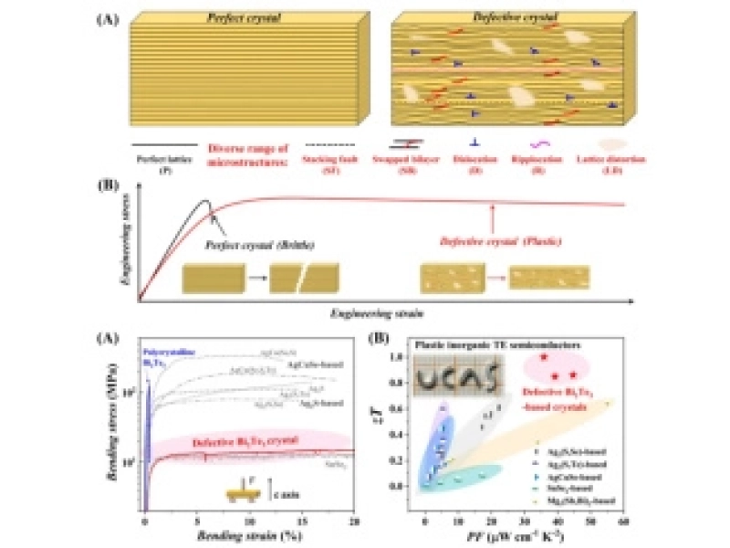
The Shanghai Institute of Ceramics publishes progress in the plasticization and regulation research of inorganic non-metallic materialsDecember/10/2024
The Shanghai Institute of Ceramics has achieved breakthrough progress in the research of high-performance thermoelectric devicesJuly/23/2025
The Shanghai Institute of Ceramics has made significant progress in the study of critical thermoelectric performanceFebruary/07/2024
The Shanghai Institute of Ceramics has achieved breakthrough progress in the research of bismuth telluride-based plastic thermoelectric materialsSeptember/26/2025
Shanghai Institute of Ceramics Achieves Major Progress in Flexible Organic/Inorganic Thermoelectric CompositesMay/26/2020